|
|
Lithography Impact on Design
to Manufacturing Flow

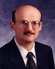
Christophe Pierrat
Numerical Technologies, San
Jose, CA
Monday, October 28, 2002, 4:00pm-5:00pm
540AB Cory Hall (DOP Center Classroom)
|
Abstract
The acceleration of the technology
roadmap and the delay of replacement options have forced lithographers
to extend the life of existing equipment. The production of 130nm technology
chips is starting using 248nm lithography instead of 193nm lithography
as was expected a few years ago. Future generations, namely 65nm, 45nm
technologies, are at risk of suffering significant delays because of their
reliance on 157nm and EUV lithography development. The widening gap between
the available tool set capability and the technical roadmap has been addressed
by increasing the numerical aperture of the projection optics and using
more aggressive resolution enhancement techniques such as model-based OPC
and alternating phase-shifting masks. The use of such techniques implies
some extensive modifications of the design to manufacturing flow as the
data sent to the mask shop does not represent the expected wafer image
anymore. In this presentation, we will review the various resolution enhancement
techniques, their insertion in the manufacturing flow, and their impact
on the chip design procedure.
Speaker
Christophe Pierrat is the director of research and development
at Numerical Technologies Inc. Before joining Numerical Technologies in
1999 he was the director of research and development at PSMC (Precision
Semiconductor Mask Corporation) from 1998 to 1999, the manager of the advanced
reticle group at Micron Technology from 1994 to 1998, and a Member of the
Technical Staff at AT&T Bell Laboratories from 1991 to 1994. He holds
a PhD from the University of Grenoble and has authored or co-authored over
60 patents and 30 technical papers.
|


